
Figure 1: Registers related to portA

Figure 2: Registers related to portB
Let's begin with ADCON0 register. This register is used to select the channel for ADC from channel 0 to channel 12 by controlling CHS3: CHS0. ADON will be used to on/off the ADC module while to determine whether the ADC conversion has completed, GO/DONE' can be checked. When GO/DONE' = 1, the ADC conversion is completed. Vice versa, when GO/DONE' = 0, this means that the A/C conversion is completed and idle.

Figure 3: ADCON0 control registers
Another important register to be taken care of when using ADC is ADCON1. This register allows to set whether the input channel will be digital or analogue by using PCFG3: PCFG0, which is bit 0 to bit bit 3 of ADCON1. VCFG1 and VCFG2 allows you to have some external voltage reference.
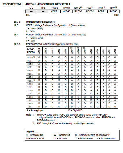
Figure 4: ADCON1 control registers
Upon setting ADCON0 and ADCON1, ADCON2 has to be set also. This register is used to control the format and the A/D acquisition time. In addition, it is also used to select the A/D conversion clock. By referring to Figure 6 and 7, the appropriate minimum acquisition time is calculated and AD clock source is chosen based on the PIC clock frequency. After doing so, then, the appropriate settings can be set.
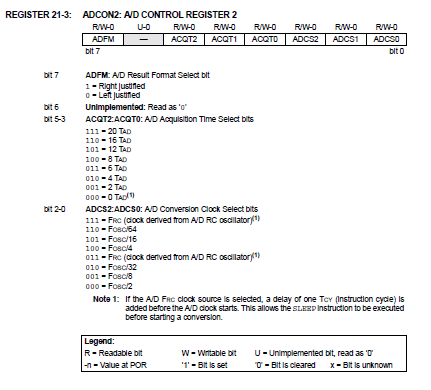
Figure 5: ADCON2 control registers

Figure 6: Equations to calculate minimum acquisition time

Figure 7: AD clock source settings
Figure 8 shows the A/D block diagram. From here, we should notice that this device's ADC has some limitation. That is, only one channel can be active at a time by controlling CHS3: CHS0. Thus, simultaneous acquiring for data more than 1 channel is impossible but parallel ADC IC can be added to perform this task.

Figure 8: A/D Diagram
Steps to configure ADC
- Configure ADC:
- Configure analogue pins, voltage references as well as digital I/O through ADCON 1
- Set A/D input channel through ADCON0 (12 channels but only one can be selected at a time)
- Select A/D time acquisition time and conversion clock through ADCON 2
- Turn on ADC through ADCON0
- If interrupt is acquired, it can be set by:
- ADIF = 0
- ADIE = 1
- GIE = 1
- Wait for acquisition time if acquired
- Start conversion by setting GO/DONE' bit in the ADCON0
- Wait for the ADC to complete by:
- Checking for the GO/DONE' bit to be cleared
- Wait for ADC interrupt
- Read the A/D Result Register ( ADRESH: ADRESL) ADIF = 0 if interrupt is used
- Go to step 1 to reconfigure another pin to acquire data or continue by going through step 3 to 5.
- A/D conversion per bit is defined as TAD.
Before the next acquisition can be done, a minimum of 3 TAD is required.
Sample coding


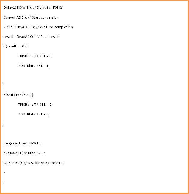

The sample code above acquires data from AN0 or channel 0 and display them to PC using serial. This is to verify that our sampling data is correct.
Conclusion
Setting up the ADC correctly is important to make sure that we acquire the correct data.
No comments:
Post a Comment